Transistor-101: Practical Common Emitter Amplifier Design
The universe started with a big-bang, just like the story of electronics started with transistors. I dedicate this page to the most common application of bipolar transistors (BJT), specifically NPN transistor. You will find a practical design and analysis of a class-A, common-emitter amplifier in this post. My favourite SPICE software is LTspice and I will use it for simulation and design verification. Ready, GO ?
Common Emitter AC Amplifier Design
First things first. Let’s see the circuit schematic for our amplifier.
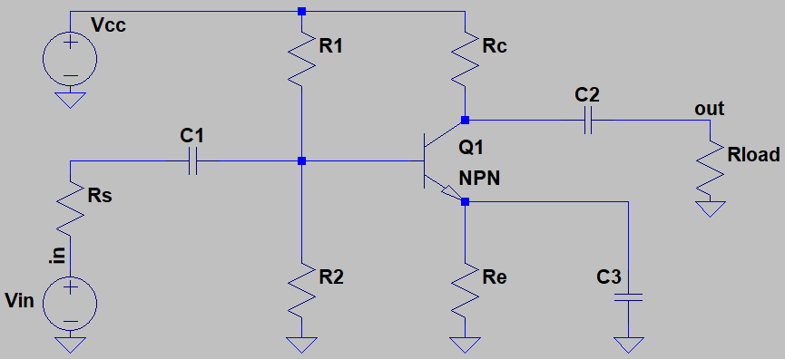
While more detailed best-practice designs exist, the circuit above is the best for teaching purposes. It works with single supply and has DC-biasing stage as well as AC-coupling elements.
Specifications
Let’s start with defining the desired input-output requirements and load conditions of the amplifier.
![]()
Transistor Selection
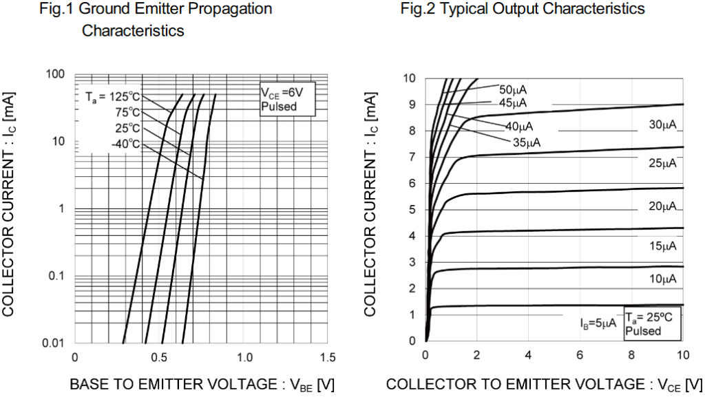
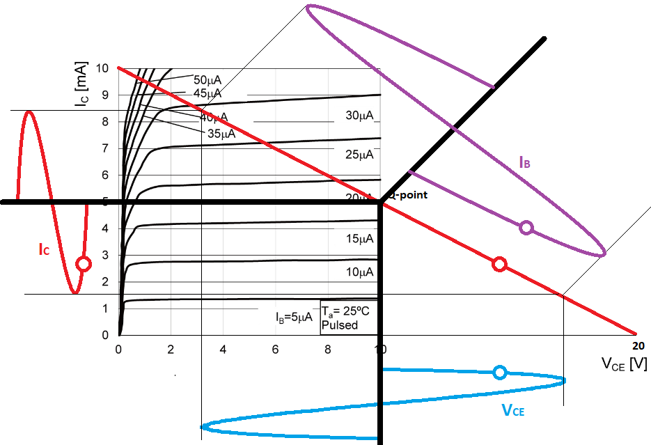
For a simple tutorial, I decided to pick a transistor that has good datasheet and good pre-installed model in LTspice. Options were limited, so i picked 2SC4102, a small current transistor from ROHM. The Base-emitter voltage and output characteristics shown below are enough information to go.
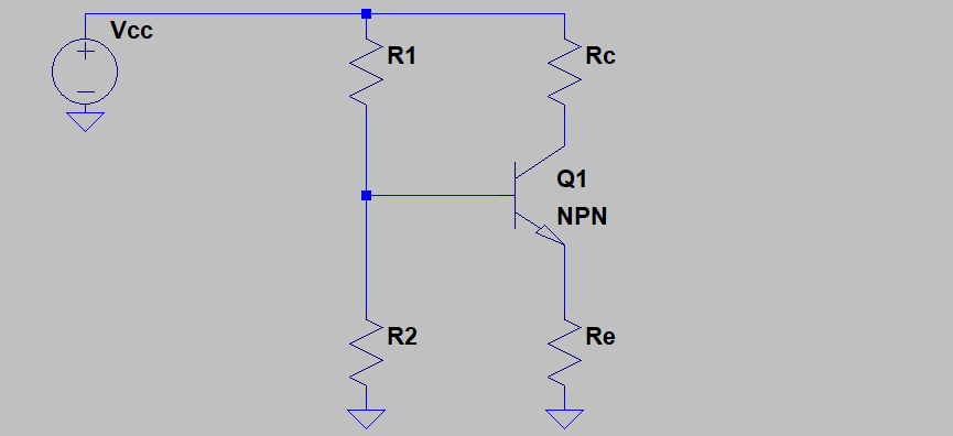
DC Bias
Class-A design requires the transistor to be in its active region even when no input signal is provided. We need to replace all capacitors with open-circuit (because of the fact that capacitors do not allow DC elements) and eliminate the unnecessary parts to have the following.
Every circuit needs a supply, so I don’t see any reason stopping us from choosing VCC=20V for this one. Secondly, we can choose the collector-emitter voltage and quiescent collector-current looking at Fig. 2. We are free to choose any point on Fig. 2 arbitrarily depending on the application, just like the following.
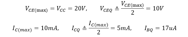
With the assumptions above, we can end up with the load-line (a.k.a. Q-point) of the amplifier.
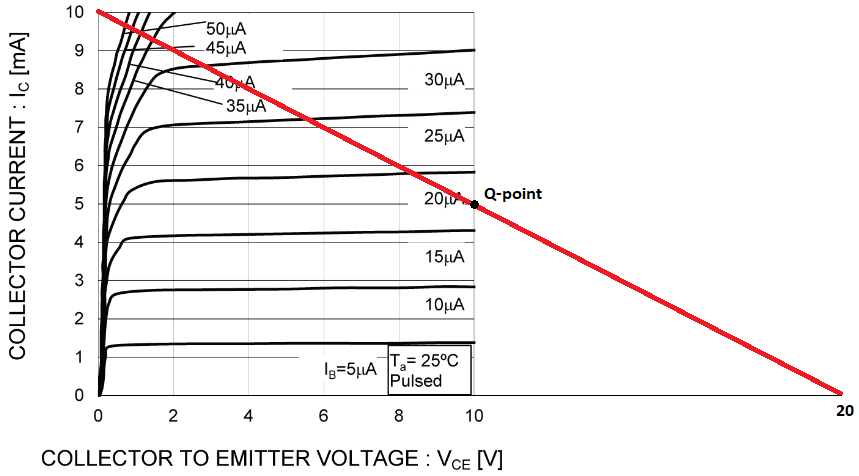
Looking at the curves, we can approximate the transistor’s gain parameter β for our desired operating-point of ICQ=5mA and VCEQ=10V. Then we can choose the voltages of collector and emitter on quiescent.
![]()
Another value we need, hidden in Fig. 1, that is VBEQ base-emitter voltage at Q-point.
![]()
This is the end of assumptions. Now we can calculate the biasing resistors R1 and R2. As a rule of thumb, we can choose R1 current as 10 times the base current and R2 current as 9 times. (Note: for high speed applications, we need to think again)

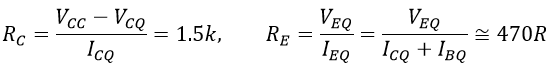
What I did here is to approximate the resistor values to the nearest 10% standard E12 resistance since these rounding does not change the operating conditions dramatically. Let’s find collector and emitter resistors.
AC Analysis
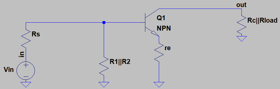
Contrary to the previous part, now we have to replace all DC voltage sources and capacitors with short-circuits (because we will choose capacitor values such that they pass the designed AC input frequency with little attenuation) to obtain the AC model of the amplifier. Result is the following.
Now let’s calculate the peak-to-peak output and base currents using Rout equivalent output resistance.

AC operation is illustrated in the following graph. When base current changes, collector current and collector-emitter voltage change respectively. It is visible that while base current and collector current increases, collector-emitter voltage decreases to cause 180* phase difference between input and output.
Note that the transistor has an intrinsic emitter resistance that is labeled as rE in the AC equivalent circuit and its approximate value depends on the thermal voltage VT (~26mV@25*C) and quiescent emitter-current IEQ. The resistance that is seen from base is β-times and input resistance depends on its value.

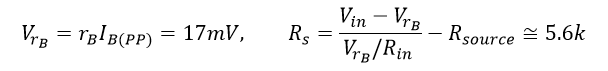
Finally, since we need to flow current of IB(PP) on intrinsic resistor rB , the voltage on rB has to be controlled with source resistor RS and Its value is calculated below.
Amplifier Gain
Theoretical gain depends only on output resistance and intrinsic emitter resistance of the designed amplifier while the overall gain is effected also by the source resistance.

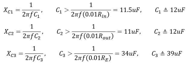
AC Coupling Capacitors
The coupling capacitors has to bypass DC biasing successfully. That is why they should be selected to have less than 1% capacitive-reactance XC than the equivalent resistances they bypass.
Simulation and Verification
With the values obtained during the design, LTspice simulation is constructed. Note that TA is set to 25*C.
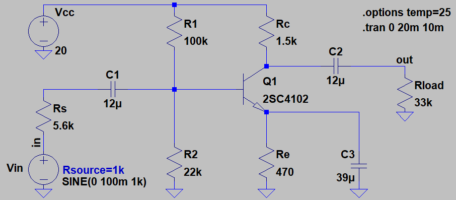
And the amplifier performance is shown below.
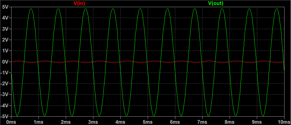 Output amplitude is ±4.9V which is very close to the desired output of ±5V and gain of -49 is very close to the calculated gain of -48. Reasons of the difference are the assumptions, approximations and model variations. It is not hard to guess that the real circuit will have bigger error.
Design Files
You can download LTspice simulation files here.
Summary
The purpose of this post was to guide you to design a basic AC amplifier. Of course there are more things to consider on the path to a successful product. Operation temperature will be a big challenge to the designer while noise and signal frequency are the other troubles. Take care until a more detailed guide ?